-
Last edited by vnrobot; 05-03-2007, 00:57. -
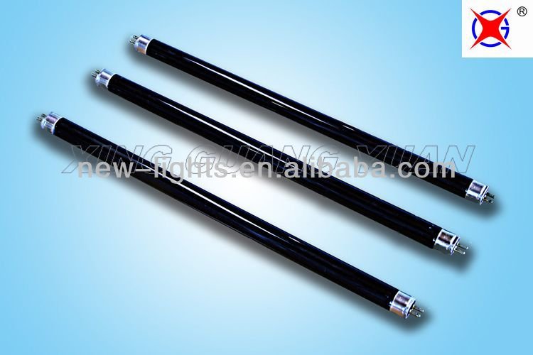
loại nào cũng ok hết, mua được đèn có bước sóng càng nhỏ càng tốt, sẽ xử lý bỏad đồng nhanh hơnNguyên văn bởi tivoi Xem bài viết
UV-A (400 - 315 ) nm
UV-B (315 - 280 ) nm
UV-C (280 - 100 ) nm
 Last edited by vnrobot; 04-03-2007, 23:47.
Comment
-
keke như vậy có đủ ko? trong công thức bác vnrobot đưa ra tí thấy có vấn đề to tát.
Cu+tia cực tím >>> cu -2e
nếu là hợp chất cao phân tử thì electron nó ko chạy tự do còn đồng thì nó dẫn điện lung tung cả .
trong 1 điều kiện mà tí chưa tìm ra vẫn có hiện tượng này xảy ra, và nó dùng đề làm bản kẽm in ofsset mà ko cấn xuất phim.
Vậy cái tuỵet chiêu này bác vnrobot làm thử chưa? có sản phẩm post lên bà con chiêm ngưỡng với
Comment
-

u sợ nó trở lại trạng thái cơ bản
ok ! chỗ này giải thích thế nào nhỉ ?Last edited by vnrobot; 05-03-2007, 01:31.Comment
-
cái gì giữ cho electron ko chạy lung tung, nói cách khác là bo đồng chĩ bị mất electrong tại điểm mà mình chiếu UV, đồng dẫn điện mử bácLast edited by tivoi; 05-03-2007, 08:10.Comment
-
theo tui thì bác vnrobot còn thiếu chất nhạy sáng nữa. Tui nghĩ phải bôi chất nhạy sáng lên board đồng trước rồi mới chiếu đèn, chớ nếu chiếu không không thì có ra cái gì đâu.
Nhưng mà nếu dùng chất nhạy sáng thì chẳng cần đèn UV gì ráo, chỉ cần nguồn sáng với cường độ mạch một chút là tốt rồi. Cái này dân in lụa rành lắm.
Tui đã từng thử rồi. nhưng gặp khó khăn là cái chất nhạy sáng này khi bị chiếu sáng rồi thì nó chẳng có dấu hiệu gì cho thấy là được hay chưa. Nghĩa là vùng bị chiếu sáng và không bị chiếu sáng chẳng khác gì nhau. chỉ khi nào ngâm mạch rồi thì mới biết kết quả, do đó mà tui đã thất bại trong thử nghiệm của mình, mạch in ra chỗ có chổ không, có lẽ do thiếu kinh nghiệm.Comment
-
không phải do bác thiếu kinh nghiệm đâu mà bác dùng keo PVA dùng cho in lụa để tráng lên bo đồng phải ko? cái loại ấy nó có bám vào kim loại đâu cho nên tay nghề bác có cao cỡ nào cũng chịu
(khi bác chụp lụa, bác dùng bóng đèn huỳnh quang nhưng thực ra mình cũng dùng cái tia cực tím do đèn huỳnh quang phát ra đó thôi, nhưng do nó yếu nên chụp lâu, dùng bóng UV sẽ nhanh hơn) còn mực UV thì trong công nghiệp IN đòi hỏi tốc độ cao nên người ta dùng đèn UV công suất lớn + bước sóng ngắn đề rút ngắn thời gian phơi UVComment
-
keo nhạy sáng
@tivoi / who_know : ?
 Vậy keo nhạy sáng nào có thể xài cho board đồng ? tên thương mại ? có thể mua ở đâu ?
 Nó có tác dụng gì trong kỹ thuật in lụa và trong việc phủ lên board Cu ?
Comment
-
hihcicic laọi mực có thể phủ lên board đồng phục vụ khắc axit thì mắc do ko thông dụng, nghe nói chỉ các nhà máy in lớn tự nhập để phục vụ làm chế bản, có chăng chỉ có mực UV thôi, mực thì chỉ phục vu in ấn thôi, ko phục vụ việc khắc axit, hic hic
cái này chắc chờ các HÓA giai việt nam nghiên cuu và phổ biến . vả lại có đi chăng nữa thì nó chỉ phục vụ in ấn là chính, ko phục vụ việc khắc axit làm chế bản. (cái này dòi hỏi dộ bền, dộ nét, và khả năng tẩy rửa sau khi khắc ...)
còn về vấn đề keo bắt sáng trong in lụa thì bác nghiên cuu trong các topic hướng dẩn làm mạch in tại gia nhé.Last edited by tivoi; 05-03-2007, 10:16.Comment
-
bài viết of tui được tham khảo ở đây
các bạn xem thử, rồi ứng dụng trong điều kiện ở VN như thế nào ?
hình như, mình thấy nó kô có đề cập đến chất gì phủ lên board Cu đâu ?
Quả thực mình kô hiểu phủ chất đó lên làm gì ?
================================================== ========
Tham khảo thêm : (kô rõ link nào)
Methods PCB fabrication
In this article we will discuss that take shape essential copper circuits via that are realized the electric connections between the elements. We will be reported extensively in the stages that it should follow the amateur but also professional electronic, in order that beginning from the theoretical diagram that has drawn in a paper it leads to what is known as printed circuit. You will still learn how it is manufactured anyone of pcb abbey or double aspect with simple and easy way. And all these following the directives that you we give below.
In order to is materialised a any printed circuit it will be supposed we begin from the designing of lines of interconnection of elements, we advance in their transport in films and we finish with the etching and the piercing of pcb. Firstly we will speak concisely for the stages of manufacture plake'tas. Then we will analyze the each one from them more extensive using photographs and drawings.
The artwork
The designing of printed circuit can become with one from the following ways:
With special thin felt-tip on rise paper or simple white paper.
With specifically designing tools (stencils) that contain islands and lines on rise paper from white paper.
With specifically design auto transferable stickers (letraset, magictype etc) in rise paper, white paper, and in special transparent gelatin.
With the help of designing programs that runs in computer, the known programs CAD, which offer facilities and crowd of possibilities.
This programs apart from the possibility simple (off-hand) transport in printer of spikes, have the possibility of printing out perfect in printers inject and laser. Certain of them have the possibility of transformation printed in form PostScript. With use of form PostScript exists the possibility of sending your drawing in special machines of photosynthesis that it is possible him they print in very high analysis in special film. In this way the final result does not have envy in nothing from a professional work. The method that has prevailed today because it has simplified all the stages is the last one. In case where the drawing of printed circuit is already ready (f.e has been published in certain periodical) then obviously we omit the stage of designing and simply we prepare the drawing for the final transport in pcb. Thus we can photocopy the drawing in rise paper or him repeat in films in some shop that has the possibility of production of special photocopies. Himself it will be supposed we make also in the other cases where the drawing has been made in paper.
The TRANSPORT of DRAWING
The transport of drawing of printed circuit above in pcb can become with a lot of ways mainest than which they are:
1. With direct designing of lines with special felt-tip indelible ink above in the copper surface pcb. This way is judged ideal for simple and small dimensions pcb or off-hand essays that should be printed out immediately.
2. With specifically auto transferable self-adhesive elements as films and islands that are stuck above in the copper surface.
3. With special self-adhesive artworks printed that is offered by certain magazines.
4. With the method that forecasts use of photosensitive special spray covering pcb (as the known Positive of 20 German company Kodakt Chemie or the Photosensitive of English company Electrolube) and film.
5. With special ready photosensitive pcb as f.e of German company Bungard. The pcb these even if they are more expensive than simple pcb have the advantage the perfect and uniform covering pcb with photosensitive material, thing that guarantees the perfect transport of drawing.
The two last methods in combination with the designing in computer give pcb high technical specifications.
EXPOSURE OF PCB IN THE UV LIGHT
The report pcb in UV light becomes in order to are burned that points that constitute the final drawing of printed circuit and will be supposed they are impressed in pcb. It is a process similar with that of appearance of photographic film. The report PCB in the UV light becomes in the interior of specifically shaped box where a special lamp of steams of mercury of force 125 W undertakes it transports the drawing printed in the surface pcb. In order to becomes possible what it will be supposed the photosensitive pcb on her adjoin film with the help of piece of pane it is placed in distance 30 hundredth from lamp UV.
Then it will be supposed it is exposed for 4 until 10 thinly depending on the type of film (gelatin, rise paper or other transparent paper) and proportionally photosensitive surface pcb. We stress that the lamp this in order to it functions needs in line with her catering a special inductor (tsok) similar with what we use in the pipes of fluorescence. If him you forget exists danger to be burned. Mark that the UV radiation is VERY DAMAGING for the eyes and should not never him you look at.
DEVELOPMENT
The appearance is the thinnest process because it requires experience and patience. It becomes with the help of special solution of 7-10 gr caustic soda (NaOH) in one liter of water. In this appears to appearance pcb for 1-2 thinly the hour. After this time becomes visible the drawing that will constitute the final electronic diagram of connections. This solution becomes denser if is added extra caustic soda. Naturally this him you will make provided that the thickness of photosensitive surface is bigger than usual. Attention: this work is imposed it becomes with plastic gloves and big attention. The caustic soda is dangerous when it comes in contact with the skin.
The ETCHING
The hour of etching is holiest for the amateur that makes this first pcb, after moment it sees his labours be rewarded. Sure it is not little you see pcb be created front in your eyes. The etching can become with four ways:
1. With solution of arid chloride iron in proportion 1:2 in water
2. With solution of chloride iron in proportion 1:1 in water
3. With solution of hythio salt of ammonia in proportion 4:10 in water in temperature 40 I C
4. With solution hydrochloric acid (2 parts) peroxide of hydrogen (perintrol 1 part) and water (4 parts)
Attention: the solution emit dangerous steams for the eyes but also for the breathing. For this reason the etching it is essential to become in open space (courtyard etc.) and never in underground or in space without good ventilation. Sure even if slow method is second. It presents the disadvantage however that where it falls this solution soils and does not leave with nothing or rather up to recently did not clean with nothing because henceforth exists in the market her dust company Bungard that will save your beloved shirt from his transformation in duster. Independent from this it is good you wear the old clothes and you avoid is poured the solution in the floor or in your skin. All the above materials you can him find in any shop of chemical products. Certain perhaps him you find also in shops electronic.
THE DRILLING
It specifically becomes with drills that accept small drills 0, 5 - 3 mms. In the practice are used drills 0,8 mms for the IC completed and drivers of elements, drills 1 mm for pins big elements, 1,2 -1,3 for pins, 1,5 for relay, switches etc and 3 mms for holes of support pcb. For better results, you can use special base of support in order to centered better the apertures. Also you can use special power supply that has the possibility of regulation turn drill but also his her force.Last edited by vnrobot; 05-03-2007, 12:17.Comment
-
Chắc bác vnrobot chưa đọc kỹ nên không thấy câu 4 nói là dùng bình xịt photosensitive để xịt lên mặt phủ đồng của miếng mạch. Còn câu 5 nói là dùng loại PCB đã được phủ sẵn chất photosensitive.Nguyên văn bởi vnrobot Xem bài viết
Cả hai loại trên đều không có thông dụng trên thị trường VN.
Chúa ơi bác đã làm bà con mừng hụt một phen. “If you create your own electricity, heating and water systems, you create your own politics. Maybe that’s what they’re afraid of.” –– Michael Reynolds
Comment
-
icic hóa ra bác chưa thử , bác xem kỹ trang bác post chưa chỗ này ne
có đoạn
The photo sensitive circuit boards will (should) be stored in a thick black bag or container. In a dark room remove one panel from the bag and seal the bag back up to protect the other panels from exposure. Remove the protective plastic film that covers the photo reactive coating.

Comment
-
lấy cái chất mà người ta tráng lên giấy rọi ảnh để xịt lên board đồng cũng được.
Hic,bác vnrobot làm em mừng hụt nhá
Comment
-
Chúa tôi !! Mình thành vật thí nghiệm từ hồi nào vậyComment
-
hihihi , ko sao bác ah, để dụng cụ đấy vẫn có tác dụng. heheh , làm sao bác làm cho các electron tren bề mặt đồng ko chạy lung tung nữa là đựơc
Last edited by tivoi; 05-03-2007, 13:18.Comment


 Tìm hiểu thêm về vnrobot

-
 Hi, một ngày mới vui vẻ và gặp nhiều may mắn, thuận lợi nhé.14-09-2026, 07:34
Comment